1. Product Basics and Structural Characteristics of Alumina Ceramics
1.1 Crystallographic and Compositional Basis of α-Alumina
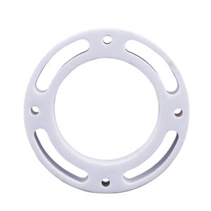
(Alumina Ceramic Substrates)
Alumina ceramic substrates, mainly composed of aluminum oxide (Al two O FOUR), work as the backbone of modern electronic packaging due to their extraordinary equilibrium of electrical insulation, thermal stability, mechanical stamina, and manufacturability.
The most thermodynamically stable stage of alumina at high temperatures is diamond, or α-Al ₂ O TWO, which takes shape in a hexagonal close-packed oxygen lattice with light weight aluminum ions occupying two-thirds of the octahedral interstitial sites.
This thick atomic setup imparts high solidity (Mohs 9), outstanding wear resistance, and strong chemical inertness, making α-alumina suitable for severe operating environments.
Commercial substratums commonly have 90– 99.8% Al Two O FIVE, with small additions of silica (SiO TWO), magnesia (MgO), or rare earth oxides used as sintering help to promote densification and control grain growth during high-temperature processing.
Greater purity qualities (e.g., 99.5% and above) exhibit exceptional electric resistivity and thermal conductivity, while lower purity variants (90– 96%) use cost-effective solutions for much less demanding applications.
1.2 Microstructure and Problem Engineering for Electronic Dependability
The performance of alumina substratums in electronic systems is seriously dependent on microstructural uniformity and flaw minimization.
A fine, equiaxed grain structure– generally varying from 1 to 10 micrometers– guarantees mechanical stability and decreases the likelihood of crack propagation under thermal or mechanical stress.
Porosity, especially interconnected or surface-connected pores, must be reduced as it breaks down both mechanical stamina and dielectric efficiency.
Advanced processing methods such as tape casting, isostatic pushing, and controlled sintering in air or managed ambiences enable the manufacturing of substratums with near-theoretical thickness (> 99.5%) and surface roughness below 0.5 µm, important for thin-film metallization and cable bonding.
In addition, pollutant partition at grain borders can cause leak currents or electrochemical migration under bias, requiring rigorous control over resources pureness and sintering problems to ensure long-term reliability in damp or high-voltage settings.
2. Manufacturing Processes and Substratum Manufacture Technologies
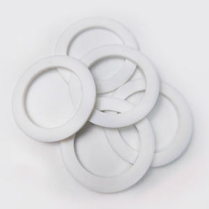
( Alumina Ceramic Substrates)
2.1 Tape Casting and Green Body Handling
The production of alumina ceramic substrates begins with the prep work of a very distributed slurry containing submicron Al ₂ O four powder, organic binders, plasticizers, dispersants, and solvents.
This slurry is refined via tape spreading– a constant technique where the suspension is topped a moving provider movie using a precision physician blade to accomplish uniform density, generally between 0.1 mm and 1.0 mm.
After solvent dissipation, the resulting “green tape” is versatile and can be punched, pierced, or laser-cut to form using holes for vertical interconnections.
Multiple layers might be laminated to produce multilayer substratums for complex circuit assimilation, although the majority of commercial applications make use of single-layer arrangements because of set you back and thermal growth considerations.
The eco-friendly tapes are after that meticulously debound to get rid of natural additives via regulated thermal disintegration prior to last sintering.
2.2 Sintering and Metallization for Circuit Combination
Sintering is carried out in air at temperature levels in between 1550 ° C and 1650 ° C, where solid-state diffusion drives pore removal and grain coarsening to attain complete densification.
The linear shrinkage throughout sintering– usually 15– 20%– must be specifically forecasted and compensated for in the style of eco-friendly tapes to make certain dimensional accuracy of the last substratum.
Following sintering, metallization is put on form conductive traces, pads, and vias.
Two key techniques dominate: thick-film printing and thin-film deposition.
In thick-film technology, pastes consisting of metal powders (e.g., tungsten, molybdenum, or silver-palladium alloys) are screen-printed onto the substrate and co-fired in a reducing atmosphere to create durable, high-adhesion conductors.
For high-density or high-frequency applications, thin-film procedures such as sputtering or dissipation are used to down payment attachment layers (e.g., titanium or chromium) adhered to by copper or gold, allowing sub-micron pattern via photolithography.
Vias are loaded with conductive pastes and discharged to establish electric affiliations between layers in multilayer styles.
3. Practical Features and Performance Metrics in Electronic Solution
3.1 Thermal and Electric Actions Under Operational Anxiety
Alumina substrates are valued for their favorable mix of modest thermal conductivity (20– 35 W/m · K for 96– 99.8% Al Two O SIX), which allows effective warm dissipation from power devices, and high quantity resistivity (> 10 ¹⁴ Ω · cm), ensuring minimal leakage current.
Their dielectric consistent (εᵣ ≈ 9– 10 at 1 MHz) is steady over a large temperature level and regularity variety, making them appropriate for high-frequency circuits up to numerous gigahertz, although lower-κ materials like aluminum nitride are preferred for mm-wave applications.
The coefficient of thermal growth (CTE) of alumina (~ 6.8– 7.2 ppm/K) is fairly well-matched to that of silicon (~ 3 ppm/K) and certain packaging alloys, lowering thermo-mechanical stress throughout device procedure and thermal biking.
However, the CTE mismatch with silicon continues to be a problem in flip-chip and straight die-attach configurations, typically requiring compliant interposers or underfill materials to reduce fatigue failing.
3.2 Mechanical Robustness and Ecological Toughness
Mechanically, alumina substratums show high flexural strength (300– 400 MPa) and superb dimensional security under load, enabling their usage in ruggedized electronics for aerospace, automobile, and industrial control systems.
They are immune to resonance, shock, and creep at elevated temperature levels, maintaining structural integrity as much as 1500 ° C in inert atmospheres.
In humid environments, high-purity alumina shows minimal moisture absorption and outstanding resistance to ion migration, guaranteeing lasting dependability in outside and high-humidity applications.
Surface firmness likewise safeguards versus mechanical damage during handling and assembly, although treatment needs to be taken to prevent edge damaging as a result of intrinsic brittleness.
4. Industrial Applications and Technological Influence Throughout Sectors
4.1 Power Electronic Devices, RF Modules, and Automotive Equipments
Alumina ceramic substrates are common in power electronic components, consisting of insulated gateway bipolar transistors (IGBTs), MOSFETs, and rectifiers, where they supply electrical seclusion while helping with warmth transfer to warmth sinks.
In radio frequency (RF) and microwave circuits, they function as provider platforms for crossbreed integrated circuits (HICs), surface acoustic wave (SAW) filters, and antenna feed networks due to their steady dielectric residential or commercial properties and low loss tangent.
In the vehicle market, alumina substrates are used in engine control units (ECUs), sensor bundles, and electric lorry (EV) power converters, where they endure heats, thermal biking, and direct exposure to harsh liquids.
Their reliability under rough problems makes them important for safety-critical systems such as anti-lock braking (ABS) and progressed motorist aid systems (ADAS).
4.2 Medical Gadgets, Aerospace, and Arising Micro-Electro-Mechanical Systems
Past customer and commercial electronics, alumina substrates are employed in implantable clinical tools such as pacemakers and neurostimulators, where hermetic sealing and biocompatibility are critical.
In aerospace and protection, they are used in avionics, radar systems, and satellite interaction modules because of their radiation resistance and stability in vacuum environments.
In addition, alumina is increasingly made use of as a structural and insulating platform in micro-electro-mechanical systems (MEMS), consisting of stress sensing units, accelerometers, and microfluidic gadgets, where its chemical inertness and compatibility with thin-film handling are beneficial.
As digital systems continue to require higher power densities, miniaturization, and reliability under extreme conditions, alumina ceramic substratums continue to be a cornerstone product, connecting the space in between efficiency, cost, and manufacturability in sophisticated electronic packaging.
5. Provider
Alumina Technology Co., Ltd focus on the research and development, production and sales of aluminum oxide powder, aluminum oxide products, aluminum oxide crucible, etc., serving the electronics, ceramics, chemical and other industries. Since its establishment in 2005, the company has been committed to providing customers with the best products and services. If you are looking for high quality alumina for sale, please feel free to contact us. (nanotrun@yahoo.com)
Tags: Alumina Ceramic Substrates, Alumina Ceramics, alumina
All articles and pictures are from the Internet. If there are any copyright issues, please contact us in time to delete.
Inquiry us